 |
LED made by RGB colors produced by the manufacturing process developed this time. Green light is when 10.8mA is flowing
Professor Fujioka Yang of the Institute of Production Technology at the University of Tokyo has developed a technology for forming LEDs by forming gallium nitride (GaN) crystals on a glass substrate by sputtering.
This technology significantly reduces the cost of substrate and crystal growth, and is expected to promote the realization of low-cost LED. In addition, there is the possibility of realizing a large-area LED at a low cost, so it is also expected to realize a large-screen high-definition LED display and a large-area LED lighting that can replace the organic EL lighting featuring surface emission.
Trial production of RGB light-emitting elements
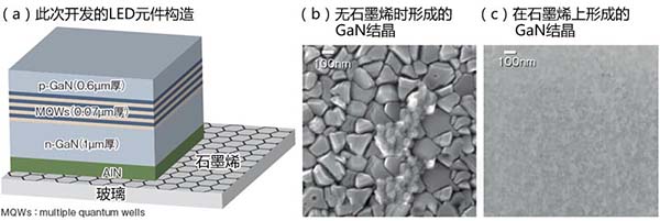
Fujioka et al. transferred a graphene multilayer film on a glass substrate of about 5 cm square. Then, AlN, n-type GaN, quantum wells (MQWs) composed of multi-layered structures of GaN and InGaN, and p-type GaN layers were formed on the graphene multilayer film by pulse sputtering (PSD) (Fig. 1 ( a)). It is said that it has been confirmed that both light excitation and current injection can be used as LED light emission. In addition, LEDs that emit light in the three primary colors of red (R), green (G), and blue (B) were also produced.
Manufacturing efficiency exceeds MOCVD
The use of sputtering to form high-quality GaN crystals, including quantum wells, was previously recognized as almost impossible, but there are still many research institutions and companies trying to develop, but "we succeed only in us, which is global It is the first time (Fujioka).
Fujioka has been working on the development of this technology since about 10 years ago. “Although the quality of GaN crystals was initially low, the quality and production efficiency have been gradually improved. Now, the production efficiency is higher than the MOCVD* commonly used in LED manufacturing, and it can also be called as Layer By Layer. Film formation at atomic unit (Fujioka) Note 1).
*MOCVD = organometallic chemical vapor deposition. Due to the need to use highly toxic organic metal raw materials and ammonia (NH3), etc., more costs are needed.
Note 1) "Sacrificial performance does not make any sense to increase manufacturing efficiency, so this time the LEDs were produced using the same film deposition rate of several micrometers per hour as MOCVD" (Fujioka).
The technology developed this time "is within the scope of experience such as crystal growth conditions and steps, and sputter devices can use existing products" (Fujioka). This technology has been used to "produce LEDs and high-electron-mobility transistors (HEMTs) made of GaN (Fujioka).
Graphene can be obtained at low cost
In addition, the reason why graphene is coated on the glass is that the crystal quality of aluminum oxide (AlN) and GaN is greatly improved (Fig. 1 (b, c)).

Figure 1: Graphene is the key to success
Structure (a) of an LED device fabricated on glass by a sputtering method developed by the Fujioka Laboratory of the University of Tokyo. It is critical that graphene is first transferred on glass, and if the graphene is not present, the quality of GaN crystals will not increase (b, c). (Image, photo provided by Tokyo University)
Fujioka developed a technique for growing AlN crystals and GaN crystals on a graphite sheet in 2008. Graphene can be a graphite sheet with only one layer of atoms. In the past three years, graphene has been able to be produced at low cost with several layers of polycrystalline graphene sheets. Graphene used this time is said to be a commercially available product. "Graphene is two-dimensional, so even if it is polycrystalline, the orientation of the c-axis is uniform and the grain boundary state is also good" (Fujioka).
In terms of the luminescent properties of LEDs, there are currently no data such as WPE (Wall Plug Efficiency) that can be compared with existing products. However, when the internal quantum efficiency of light excitation under extremely low temperature conditions is detected, "the result is lower than that of existing LEDs. The future problem is how to improve internal quantum efficiency" (Fujioka).
Can also be manufactured on large areas of glass
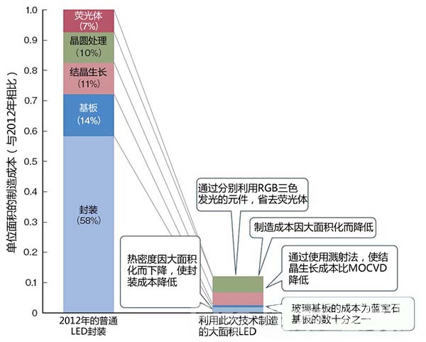
If the luminescence performance is not a big problem, this technology may shake the existing LED technology, and even LCD and organic EL technology (Figure 2).

Figure 2: The price of large-area LEDs approaches the original 1/10
The estimated value of the manufacturing cost per unit area when manufacturing large area LEDs using this technology is compared with the 2012 average LED package. The cost per unit area approaches the original 1/10. Assuming that the cost of crystal growth is reduced to 1/2 by using sputtering, the manufacturing cost of wafer processing is also reduced to 1/2 due to the large area.The specific cost in 2012 is based on the US Department of Energy data.
First, by changing the substrate to glass, the LED's sapphire substrate is eliminated. The cost of a glass substrate is only one tenth of that of a sapphire substrate. Even if compared with "GaNon-Si" technology that uses a Si substrate that is cheaper than sapphire, lower costs are expected to be realized. Furthermore, by using the sputtering method, the cost of the crystal growth apparatus is also lower than that of the MOCVD method. In addition, if the RGB light-emitting elements can be manufactured separately, the cost of the phosphor can also be saved. However, with these improvements alone, LED manufacturing costs have also dropped by less than 1/2. Because the cost of packaging accounts for 60% of the total.
In response, Fujioka believes that "the high cost of LED packaging is due to the cost of heat dissipation by flowing large currents through small LED chips. Sputtering is also commonly used to make liquid crystal displays on glass with several square meters." It is suitable for large-area film formation. In this way, the packaging cost can be greatly reduced when manufacturing large-area LEDs." At this time, the manufacturing cost per unit area is close to 1/10 of the existing LED.
If a large-area LED can be manufactured at a low cost, the threshold will be greatly reduced when realizing a self-luminous LED display without using a liquid crystal. And compared with organic EL, it also has the advantage of high reliability.
Although a glass substrate was used this time, "as long as the graphene can be transferred and has a heat resistance that can withstand a processing temperature of about 500C, any material can be used for the substrate" (Fujioka). In addition, if an ultra-thin flexible glass substrate or the like is used, a large-area LED having flexibility can also be manufactured. (Reporter: Nozawa Tetsuru, Nikkei Electronics)
Led Headlamp,Head Lamp,Led Car Headlights,Led Mining Headlamp
Cangnan Younglite Electrical Co., Ltd. , https://www.younglitelight.com