Research on back polishing technology of monocrystalline silicon solar cells (1)
As one of the five most important areas of economic development in the 21st century, solar power is one of the new energy and renewable energy sources. Because of its environmental protection, high efficiency, energy saving, and inexhaustible use, solar power generation Exhaustion and other characteristics have become the most attractive energy source in new energy. Therefore, efforts to strengthen the research and development of solar cells and other photovoltaic industries, and continuously improve the photoelectric conversion efficiency has become the key to win in the fierce market competition in the future, and continue to promote the technological progress of the photovoltaic industry and promote the application in larger scale. The crystalline silicon solar cell is At present, the mainstream of the photovoltaic industry, in order to improve the competitiveness of enterprises in the market, to improve the conversion efficiency of crystalline silicon solar cells is imminent.
Conventional single crystal silicon solar cells use chemical methods to texture the surface of the suede due to the need for light trapping, increasing the surface area and reducing the reflectance by reflecting/absorbing light. However, the presence of suede also has a negative effect, and the position of the deep surface of the suede is in contact with the metal. Therefore, we consider polishing the back surface of the silicon wafer to make the back surface of the silicon wafer smoother or even mirror-finished. After the back polishing, the back surface of the silicon wafer is flat. On the one hand, the reflection of transmitted light can be enhanced to reduce the light transmittance. The aluminum paste can be brought into contact with the surface of the silicon wafer to further improve the passivation effect.
The current density Jsc and the open circuit voltage Uoc are improved by the back surface polishing, so that the conversion efficiency of the solar cell can be improved. This paper verifies this by means of experimental means.
1 solar cell and process
The basic structure of a crystalline silicon solar cell is shown in Figure 1. The base material is p-type crystalline silicon with a thickness of about 200 μm. The upper surface is a layer of n+-type diffusion region, which together with the matrix forms the basic structure of the photovoltaic effect--pn Knot
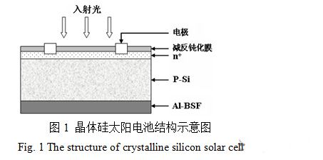
The entire upper surface is evenly covered with the anti-passivation film; the top surface has a grid-shaped front electrode, and the back surface is screen-printed and sintered to form an aluminum-covered back surface electric field BSF (BackSurfaceField) and a back electrode, and the positive electrode The n+ region contacts, and the BSF and the back electrode form an ohmic contact with the p region, and the production flow is shown in Fig. 1.A.
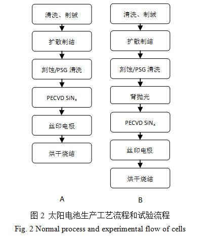
This experiment is based on the traditional process to increase the back polishing process (Figure 2.B).
Measuring Tape,Smart Measuring Tape,Mini Measuring Tape,Retractable Measuring Tape
Shangqiu Hengli Measuring Tools Co.,Ltd , https://www.henglimtools.com