The Chinese Academy of Sciences announced today that domestic scholars have developed a simple method for preparing low-dimensional semiconductor devices-using "nano brushes" to outline future optoelectronic devices, which can "draw" various required chips. With the development of technology, people have higher and higher requirements for semiconductor technology, but the difficulty of semiconductor manufacturing is getting greater and greater. The process below 10nm is extremely burning money, which requires other technologies.
The Chinese Academy of Sciences said that in the foreseeable future, more electronic components need to be integrated in a smaller area. In response to this demand, low-dimensional materials with a thickness of only 0.3 to a few nanometers (tens of thousands of hair diameters) came into being.
This type of material can be compared to ultra-thin paper, but it is much thinner than paper, and can be used to prepare nano-level electronic devices.
From the material to the device, the existing preparation process needs to go through a very complicated and complicated process, which is extremely disadvantageous for the rapid screening of low-dimensional materials suitable for preparing electronic devices.
Recently, researchers from the Shanghai Institute of Technical Physics of the Chinese Academy of Sciences have developed a simple method for preparing low-dimensional semiconductor devices-using "nano brushes" to outline future optoelectronic devices.
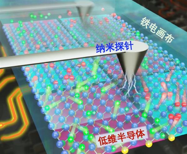
Since the two-dimensional material is like a thin piece of paper, its properties are easily affected by the environment. Using this feature, the researchers covered a layer of ferroelectric thin film on the surface of the two-dimensional material, used a nanoprobe to apply a voltage to scan the surface of the ferroelectric material, and changed the properties of the ferroelectric material at the corresponding position to achieve the accuracy of the properties of the two-dimensional material. Manipulation.
After designing the device functions, researchers only need to use their imagination to draw various electronic device patterns on the "canvas" of the ferroelectric thin film using the nano-probe "brush", and use the ferroelectric thin film to physics of low-dimensional semiconductor materials. Influence of the nature, can make the required device.
In actual experimental operation, the "brush" is a nanoprobe of an atomic force microscope. Its function is equivalent to the gate electrode of a traditional transistor, which can be used to apply positive or negative voltage.
But unlike traditional grid electrodes, the tip of an atomic force microscope can be moved arbitrarily, like a "walking paintbrush", which can accurately "draw" nano-scale devices in horizontal space.
In this process, researchers can easily construct various electronic and photonic devices, such as memories, photodetectors, photovoltaic cells, etc., by controlling the positive and negative voltages applied to the needle tip.

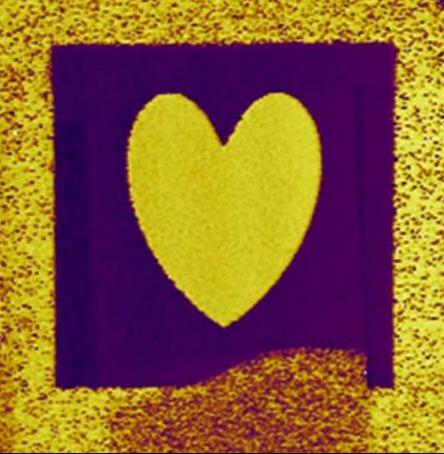
The picture below is a heart-shaped pattern written with the tip of a probe, which fully reflects the arbitrariness of graphic editing.
Moreover, after a device is written, it can be scanned with a different voltage using the tip of the needle, and it can also be written as a new functional device, just like writing on paper and then using an eraser to clean and rewrite, that is, the same device can be repeated Use and realize different functions.
Just like a robot, refreshing the control program can do different things.

Researchers have further applied this probe scanning technology to quasi-nonvolatile memory.
Quasi-non-volatile memory refers to a type of memory that satisfies both the faster write data speed and the longer time to save data. It makes sense to develop this type of storage technology. For example, it can extend the time that data is saved when we shut down the computer or shut down the computer suddenly or unexpectedly.
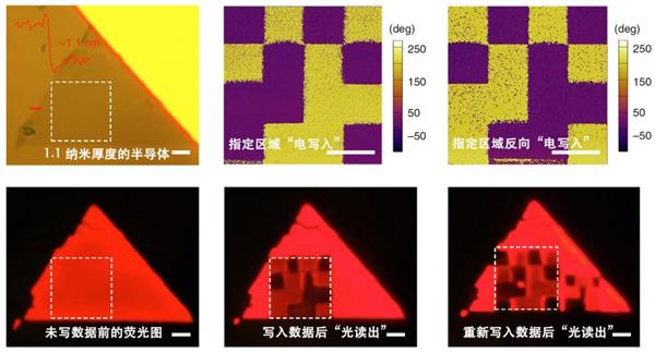
In addition, this device preparation technology can also be used to design "electrical writing, optical readout" memory, the CD-ROM we use daily is a typical "optical readout" storage medium.
Because the type of low-dimensional semiconductor carrier will change under the action of the scanning electric field at the tip, this will result in a significant change in its luminous intensity.
Therefore, combined with the characteristics of arbitrary editing of scanned graphics, researchers can design arrays that change periodically.
Each area of ​​these array patterns passes through the tip of the needle to control its carrier type, which in turn controls the luminous intensity of the low-dimensional material, and then a photo taken with a camera can directly obtain a photo of fluorescence intensity.
The information of each storage unit is "at a glance" in this photo. The dark unit can be used to represent the "0" in the storage state, and the bright unit can be used to represent the "1", similar to a new type of storage "CD" ".
Researchers can obtain the information of each storage unit at the same time simply and directly by taking fluorescent photos.
Using this technology, if the voltage is read out, the theoretical storage density can reach several T-Byte / in2.

This research was carried out in collaboration with several research groups including the Shanghai Institute of Technical Physics, the Chinese Academy of Sciences, Fudan University, East China Normal University, Nanjing University, and the Institute of Microelectronics, Chinese Academy of Sciences.
The research results have been published in "Nature-Electronics" on January 24, 2020. The article title is "Programmable transition metal dichalcogenide homojunctions controlled by nonvolatile ferroelectric domains".
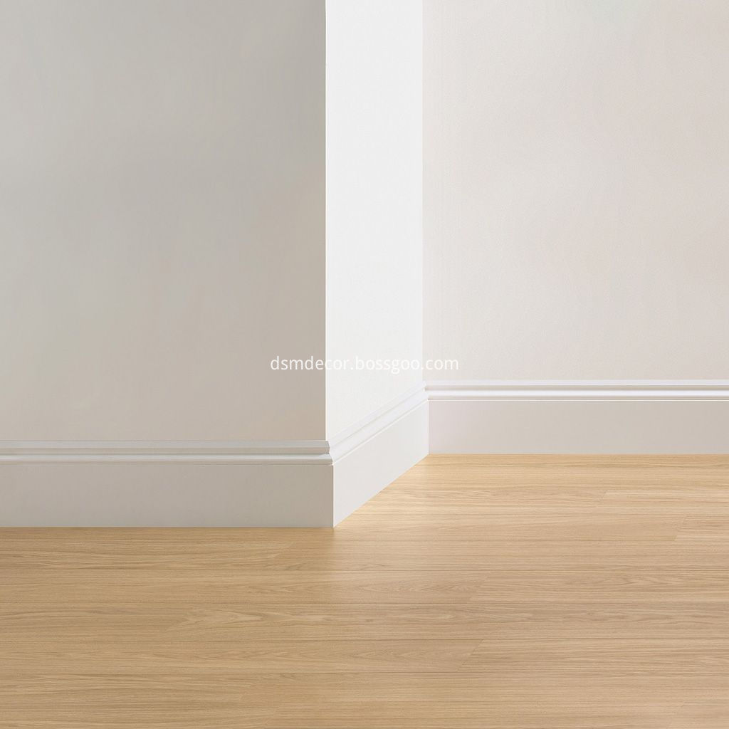
PU Floor Profiles are widely used to decorate at the foot base of the wall.
Without PU Floor Profiles, the transition from floor to wall looks unfinished and bare and allows walls to be easily damaged. Skirting boards are more than just decoration. It protects the wall, hides cracks and sometimes also covers expansion areas for parquet floors. You can choose the skirting board that matches the architecture of the room with your own style and size of the room. You can paint it(Floor Skirting,Skirting Boards,Aluminum Floor Profiles,Floor Trim Profiles,Baseboard Moulding,wall baseboard) to achieve the perfect color with other decorations.
Advantages:
1. Elegant European style
2. Many models to choose from
3. Suitable for both DIY and construction projects
4. Superior to Gypsum moldings
5. Light weight, easy to transport and install
6. Elaborate patterns
7. Better flexibility
8. Labor efficient
Our Service:
1. Factory direct sale with excellent quality, reasonable price and first-class service.
2. Timely delivery to every corner of the world.
3. Strong supply capacity, high-tech skills and advanced equipment can surely meet customers` requirement.
4. Launching new designs for each category every year.
5. Exquisite workmanship. All products 100% inspected.
6. Preferential freight by Famous shipping company.
7. Excellent after-sales service

Floor Profiles,Floor Skirting,Skirting Boards,PU Skirting Boards,Pu Skirtings,Pu baseboards,Wall Baseboards
Suntronic New Materials Technology Co., Ltd. , https://www.dsmdecor.com